In preparation
35. FiND: Few-shot three-dimensional image-free confocal focusing on point-like emitters

Confocal fluorescence microscopy is widely applied for the study of point-like emitters such as biomolecules, material defects, and quantum light sources. Confocal techniques offer increased optical resolution, dramatic fluorescence background rejection, and sub-nanometer localization, useful in superresolution imaging of fluorescent biomarkers, single-molecule tracking, or the characterization of quantum emitters. However, rapid, noise robust automated 3D focusing on point-like emitters has been missing for confocal microscopes. Here, we introduce FiND (Focusing in Noisy Domain), an imaging-free, non-trained 3D focusing framework that requires no hardware add-ons or modifications. FiND achieves focusing for signal-to-noise raios down to 1, with a few-shot operation for signal-to-noise ratios above 5. FiND enables unsupervised, large-scale focusing on a heterogeneous set of quantum emitters. Additionally, we demonstrate the potenIal of FiND for real-time 3D tracking by following the drift trajectory of a single NV center indefinitely with a positional precision of < 10 nm. Our results show that FiND is a useful focusing framework for the scalable analysis of point-like emitters in biology, material science, and quantum optics.
S. Sahoo, J. Jiang, J. Li, K. Loehr, C.E. Germany, J. Zhou, B.K. Clark, and S.I. Bogdanov, preprint available on arXiv at https://arxiv.org/abs/2311.06479
34. T-fluctuations and dynamics of the resistive transition in thin superconducting films
We investigate the temporal and spatial scales of resistance fluctuations (R-fluctuations) at the superconducting resistive transition in thin epitaxial TiN films, accessed through voltage fluctuation measurements in current-biased samples. The measured Lorentzian spectrum of the R-fluctuations identifies their correlation time, which is shown to coincide with the thermal relaxation time determined by a combination of the electron-phonon relaxation and the diffusion in reservoirs. Our data is quantitatively consistent with the model of spontaneous temperature fluctuations, the Tfluctuations, with a variance given by the textbook thermodynamic expression. We discuss the experimental indication that the T-fluctuations contribute to the broadening of the transition, in spite of vanishing in the limit of infinite sample volume. Our observations highlight important caveats in the accepted physical picture of the resistive transition.
E.M. Baeva, A.I. Kolbatova, N.A. Titova, S. Saha, A. Boltasseva, S.I. Bogdanov, V.M. Shalaev, A.V. Semenov, A. Levchenko, G.N. Goltsman, and V.S. Khrapai, preprint available on arXiv at https://arxiv.org/pdf/2202.06309
Published articles
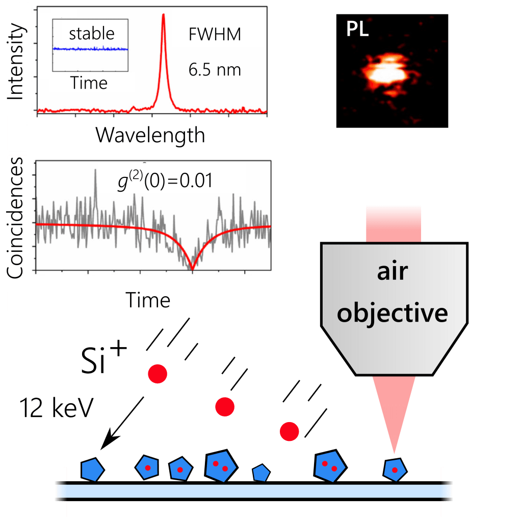
33. Ultranarrow Bright Single-Photon Emitters in Diamond with Strong Broadband Phonon Decoupling
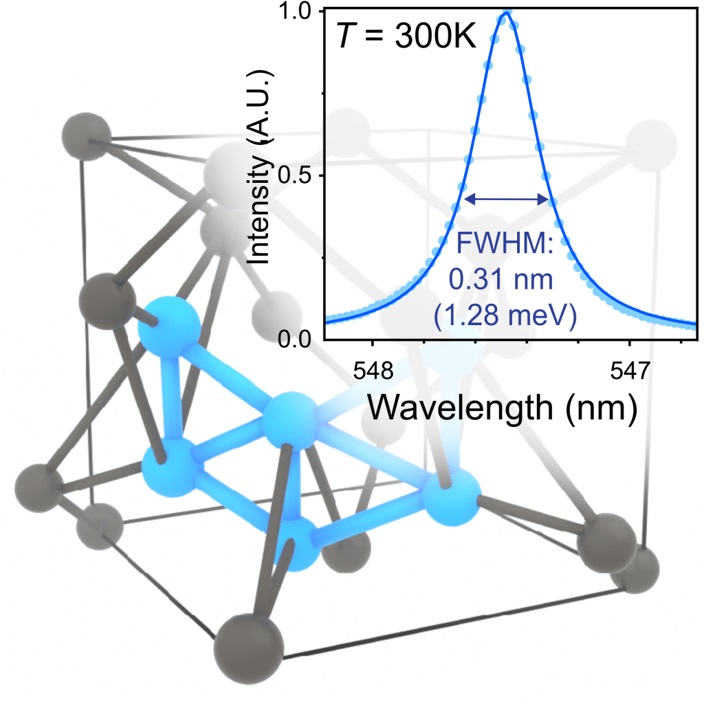
Single-photon emitters are fundamental building blocks for quantum information processing, communication and sensing. However, unwanted interactions with bulk phonons in their host environment strongly limit their coherence and controllability. We report single color centers in nanodiamonds that are strongly and comprehensively decoupled from the bulk phononic environment. The color centers feature record-narrow linewidths down to 0.3 nm at room temperature and stable, bright emission, exceeding 10 Mcps in saturation. Notably, the bulk phonon sideband is almost entirely suppressed, revealing the presence of a single localized vibrational mode outside the diamond phonon band. Our observations and simulations point towards a unique mechanism for phonon decoupling in common wide-gap materials, based on a strongly radiative orbital transition coupled to a localized vibrational mode. The new color center enables qualitatively higher performance for applications in quantum networks and nanoscale sensing, and the exploration of new physical resources associated with vibrational states.
S. Sahoo, P. Udvarhelyi, J. Li, D. Kim, V. Agafonov, V. A. Davydov, B. Lawrie, P. Narang, and S.I. Bogdanov, Nat. Commun. (2026)
32. Remote plasma for damage-controlled fabrication of singlephoton emitters in ultrathin hexagonal boron nitride
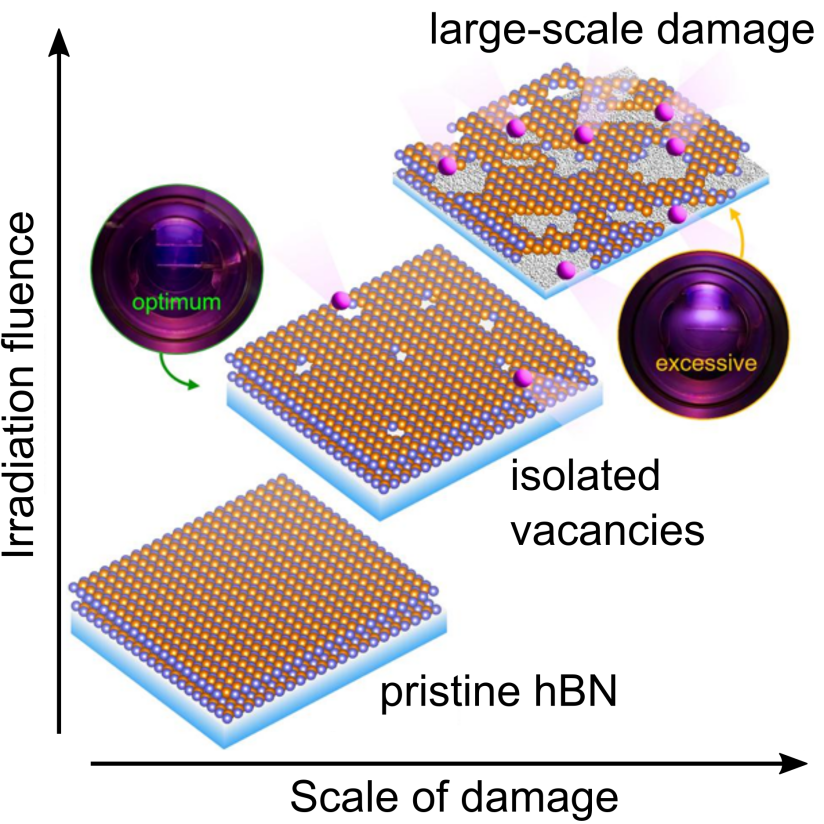
Hexagonal boron nitride (hBN) hosts bright and robust color centers, with emission in the ultraviolet to near-infrared range, that are generally obtained either by activating pre-existing atomic defects or by purposefully introducing strain, vacancies, or impurities. Controlled fabrication remains a challenge as color centers often form on extended structural defects, including pre-existing flake edges, holes, and folds, as well as unintended damage sites created during vacancy generation. Here, we introduce a remote argon plasma technique to produce vacancies while minimizing material damage. Additionally, by independently tuning the ion flux and energy, we engineer large arrays of single-photon emitters (SPEs). Critically, the SPEs form away from nanoscale non-uniformities, in pristine flake regions. Our processing approach thus enables the formation of stable SPEs with bulk properties in atomically thin hBN. The noninvasive formation of color centers in 2D materials opens multiple pathways toward their applications in sensing and quantum photonics.
S. Bhattacharya, S. Sahoo, H. Dong, D.H. Hong, T. Taniguchi, K. Watanabe, N. Mason, A. van der Zande, S.I. Bogdanov and R.M. Sankaran Appl. Phys. Lett. 128, 214103 (2026)
31. Low-temperature electron dephasing rates indicate magnetic disorder in superconducting TiN films
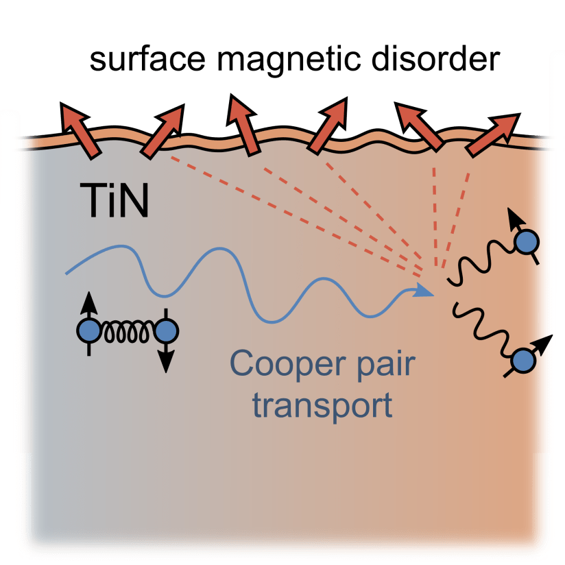
We investigate electron transport and phase-breaking processes in thin titanium nitride (TiN) films of epitaxial quality. Previous studies show that a minute surface magnetic disorder significantly reduces the critical temperature (Tc) and broadens the superconducting transition as the film thickness and device size decrease. We measure electron dephasing rates via magnetoresistance from Tc to 4Tc in various-thickness TiN films. Electron dephasing occurs on the picosecond timescale and is nearly independent of temperature, differing from the expected inelastic scattering due to the electron–phonon and electron–electron interactions near Tc, which occur over a nanosecond timescale. We propose spin-flip scattering as a possible additional phase-breaking mechanism. The significant increase in the dephasing rate for the thinnest film indicates that magnetic disorder resides near the surface of naturally oxidized films. Our research suggests that magnetic disorder may be a significant contributor to RF dissipation in superconducting devices based on TiN.
A. I. Lomakin, E. M. Baeva, N. A. Titova, A. V. Semenov, A. V. Lubenchenko, M. A. Kirsanova, S. A. Evlashin, S. Saha, S. Bogdanov, A. I. Kolbatova, and G. N. Goltsman, Appl. Phys. Lett. 127, 173501 (2025)
30. Fast quantum interferometry at the nanometer and attosecond scales with energy-entangled photons
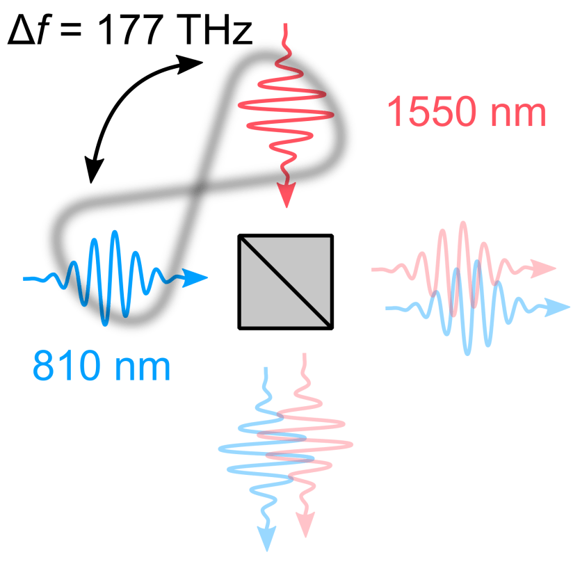
In classical optical interferometry, loss and background complicate achieving fast nanometer-resolution measurements with illumination at low light levels. Conversely, quantum two-photon interference is unaffected by loss and background, but nanometer-scale resolution is physically difficult to realize. As a solution, we enhance two-photon interference with highly nondegenerate energy entanglement featuring photon frequencies separated by 177 THz. We observe measurement resolution at the nanometer (attosecond) scale with only O(104) photon pairs, despite the presence of background and loss. Our nondestructive thickness measurement of a metallic thin film agrees with atomic force microscopy, which often achieves better resolution via destructive means. With contactless, nondestructive measurements in seconds or faster, our instrument enables metrological studies in optically challenging contexts where background, loss, or photosensitivity are factors.
C. Lualdi, S. Johnson, M. Vayninger, K. Meier, S. Sahoo, S.I. Bogdanov, and P.G. Kwiat Sci. Adv., 11, eadw4938 (2025)
29. Natural width of the superconducting transition in epitaxial TiN films
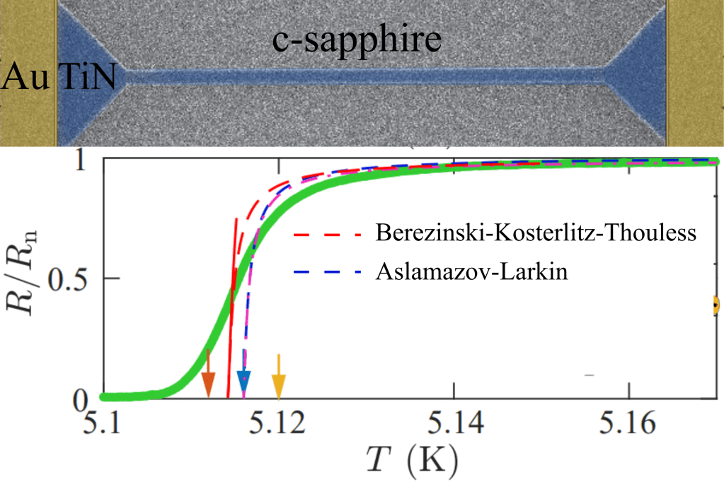
We investigate the effect of various fluctuation mechanisms on the dc resistance in superconducting devices based on epitaxial titanium nitride (TiN) films. The samples we studied show a relatively steep resistive transition (RT), with a transition width δT/Tc ~ 0.002-0.025, depending on the film thickness (20 nm, 9 nm, and 5 nm) and device dimensions. This value is significantly broader than expected due to conventional superconducting fluctuations ( δT/Tc < 10-3). The shape and width of the RT can be perfectly described by the well-known effective medium theory, which allows us to understand the origin of the inhomogeneity in the superconducting properties of TiN films. We propose that this inhomogeneity can have both dynamic and static origins. The dynamic mechanism is associated with spontaneous fluctuations in electron temperature (T-fluctuations), while the static mechanism is due to a random spatial distribution of surface magnetic disorder (MD). Our analysis has revealed clear correlations between the transition width and material parameters as well as device size for both proposed mechanisms. While T-fluctuations may contribute significantly to the observed transition width, our findings suggest that the dominant contribution comes from the MD mechanism. Our results provide new insights into the microscopic origin of broadening of the superconducting transition and inhomogeneity in thin superconducting films.
E.M. Baeva, A.I. Kolbatova, N.A. Titova, S. Saha, A. Boltasseva, S.I. Bogdanov, V.M. Shalaev, A.V. Semenov, G.N. Goltsman, and V.S. Khrapai, Supercond. Sci. Technol. 37 105017 (2024)
28. Terahertz-mediated microwave-to-optical transduction
Transduction of quantum signals between the microwave and the optical ranges will unlock powerful hybrid quantum systems enabling information processing with superconducting qubits and low-noise quantum networking through optical photons. Most microwave-to-optical quantum transducers suffer from thermal noise due to pump absorption. We analyze the coupled thermal and wave dynamics in electro-optic transducers that use a two-step scheme based on an intermediate frequency state in the THz range. Our analysis, supported by numerical simulations, shows that the two-step scheme operating with a continuous pump offers near-unity external efficiency with multi-order noise suppression compared to direct transduction. As a result, two-step electro-optic transducers may enable quantum noise-limited interfacing of superconducting quantum processors with optical channels at MHz-scale bitrates.
F. Sahbaz, J. Eckstein, D. van Harlingen, and S.I. Bogdanov, Phys. Rev. A 109, 042409 (2024)
27. Machine learning assisted quantum super-resolution microscopy

One of the main characteristics of optical imaging systems is the spatial resolution, which is restricted by the diffraction limit to approximately half the wavelength of the incident light. Along with the recently developed classical superresolution techniques, which aim at breaking the diffraction limit in classical systems, there is a class of quantum super-resolution techniques which leverage the non-classical nature of the optical signals radiated by quantum emitters, the so called antibunching super-resolution microscopy. This approach can ensure a factor of √𝑛 improvement in the spatial resolution by measuring the 𝑛 -th order autocorrelation function. The main bottleneck of the antibunching super-resolution microscopy is the time-consuming acquisition of multi-photon event histograms. We present a machine learning-assisted approach for the realization of rapid antibunching super-resolution imaging and demonstrate 12 times speed-up compared to conventional, fitting-based autocorrelation measurements. The developed framework paves the way to the practical realization of scalable quantum super-resolution imaging devices that can be compatible with various types of quantum emitters.
Z.A. Kudyshev, D. Sychev, Z.O. Martin, S.I. Bogdanov, X. Xu, A.V. Kildishev, A. Boltasseva and V.M. Shalaev, Nat. Commun., 14, 4828 (2023).
26. Fabrication of single color centers in sub-50 nm nanodiamonds using ion implantation
Diamond color centers have been widely studied in the field of quantum optics. The negatively charged silicon vacancy (SiV) center exhibits a narrowband efficient emission at 738 nm, and unique spin properties, making it a promising emitter for quantum information technologies and bioimaging. In particular, nanodiamond (ND)-based SiV centers can be heterogeneously integrated with plasmonic and photonic nanostructures and serve as in vivo biomarkers and intracellular thermometers. We report the creation of single color centers featuring high-purity single-photon emission through Si implantation into ~ 20 nm size NDs. We observe room-temperature emission with linewidths below 10 nm and center wavelengths spanning the range of 730 – 800 nm. Ion implantation uniquely promises the controllable creation of color centers in preselected individual NDs, with applications in quantum photonics, sensing and biomedicine.
X. Xu, Z.O. Martin, M. Titze, Y. Wang, D. Sychev, J. Henshaw, A.S. Lagutchev, H. Htoon, E.S. Bielejec, S.I. Bogdanov, V.M. Shalaev and A. Boltasseva, Nanophot., 13, 1 (2023)
25. Hybrid quantum nanophotonic devices with color centers in nanodiamonds
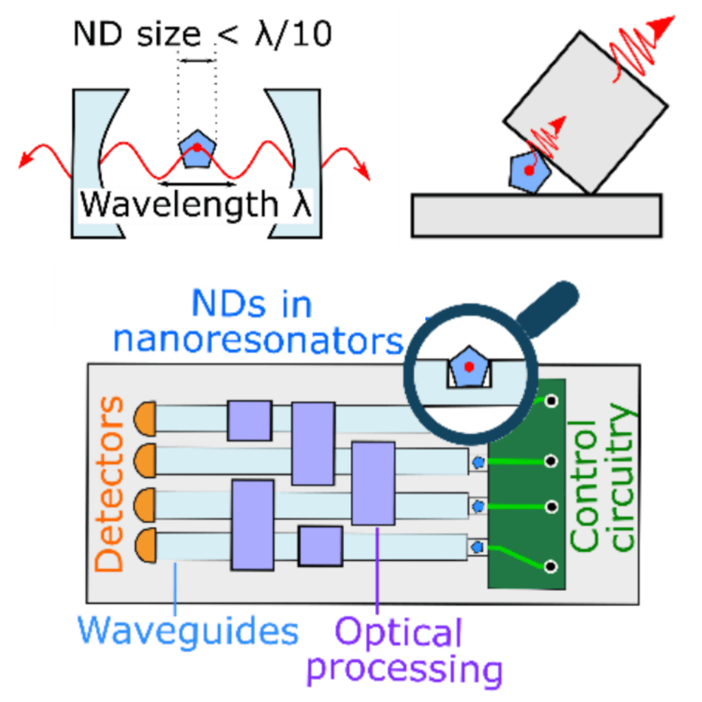
Optically active color centers in nanodiamonds offer unique opportunities for generating and manipulating quantum states of light. These mechanically, chemically, and optically robust emitters can be produced in mass quantities, deterministically manipulated, and integrated with a variety of quantum device geometries and photonic material platforms. Nanodiamonds with deeply sub-wavelength sizes coupled to nanophotonic structures feature a giant enhancement of light-matter interaction, promising high bitrates in quantum photonic systems. We review the recent advances in controlled techniques for synthesizing, selecting, and manipulating nanodiamond-based color centers for their integration with quantum nanophotonic devices.
S. Sahoo, V.A. Davydov, V.N. Agafonov, and S.I. Bogdanov, Opt. Mater. Exp., 13, 191 (2023)
24. Electric field control of interaction between magnons and quantum spin defects

The nanoscale magnetic field of magnons has emerged as a promising resource for coherently driving qubits such as quantum spin defects (QSD) and developing versatile probes for magnetism and other types of quantum matter. Tuning this coupling via electric field would provide a path to address the outstanding challenges of enhancing QSD-based sensing of electric fields and locally manipulating QSD qubits with minimal power. Here, we demonstrate a new approach to such electric field tuning using a ferromagnet-ferroelectric hybrid multiferroic film integrated with nitrogen-vacancy (NV) center spins. Combining NV-spin relaxometry with ferromagnetic resonance measurements, we reveal that the ferroelectric polarization controls the magnetic anisotropy, which tunes the magnon-generated fields at the NVs. Flipping the ferroelectric polarization changes NV-spin relaxation rate by 400%, which could be further enhanced by three orders of magnitude by nanopatterning the ferromagnets. Our results offer possibilities of realizing improved NV-sensing of electric fields, electric-field-tunable quantum spintronic devices, and magnon/spin probes of the multiferroic order and quantum materials.
A.B. Solanki, S.I. Bogdanov, M.M. Rahman, A. Rustagi, N.R. Dilley, T. Shen, W. Tong, P. Debashis, Z. Chen, J. Appenzeller, Y.P. Chen, V.M. Shalaev, and P. Upadhyaya, Phys. Rev. Research, 4, L012025 (2022)
23. Rapid absolute sizing of deeply subwavelength dielectric nanoparticles by confocal scanning optical microscopy
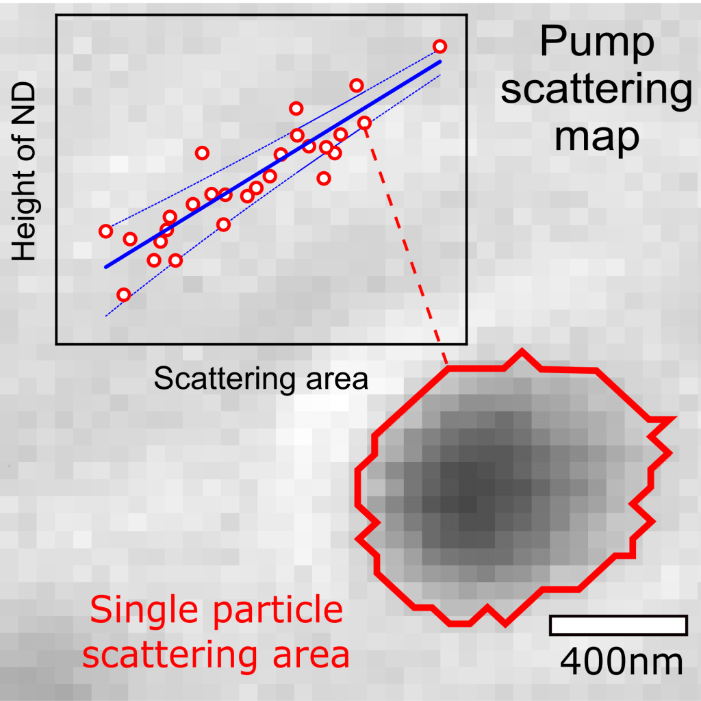
Accurate sizing of individual nanoparticles is crucial for the understanding of their physical and chemical properties, and for their use in nanoscale devices. Optical sizing methods are noninvasive, rapid and versatile. However, the low optical response of weakly absorbing subwavelength dielectric nanoparticles poses a fundamental challenge for their optical metrology. We demonstrate scalable optical sizing of such nanoparticles based on confocal scanning microscopy. The method is absolutely calibrated by correlating the optical signatures in the scattered pump laser signal to the ground truth nanoparticle sizes measured by an atomic force microscope. Using an air objective with a numerical aperture of 0.9, we measured the sizes of nanodiamond particles ranging from 35 to 175 nm, with an average error of ± 12.7 nm compared to the ground truth sizes. This technique paves the way for the metrology of a wide range of weakly scattering nano-objects for applications in biomedicine, catalysis, nanotechnology and quantum optics.
S. Sahoo, H. Azzouz, and S.I. Bogdanov, Appl. Phys. Lett. 118, 241105 (2021)
22. Rapid classification of quantum sources enabled by machine learning
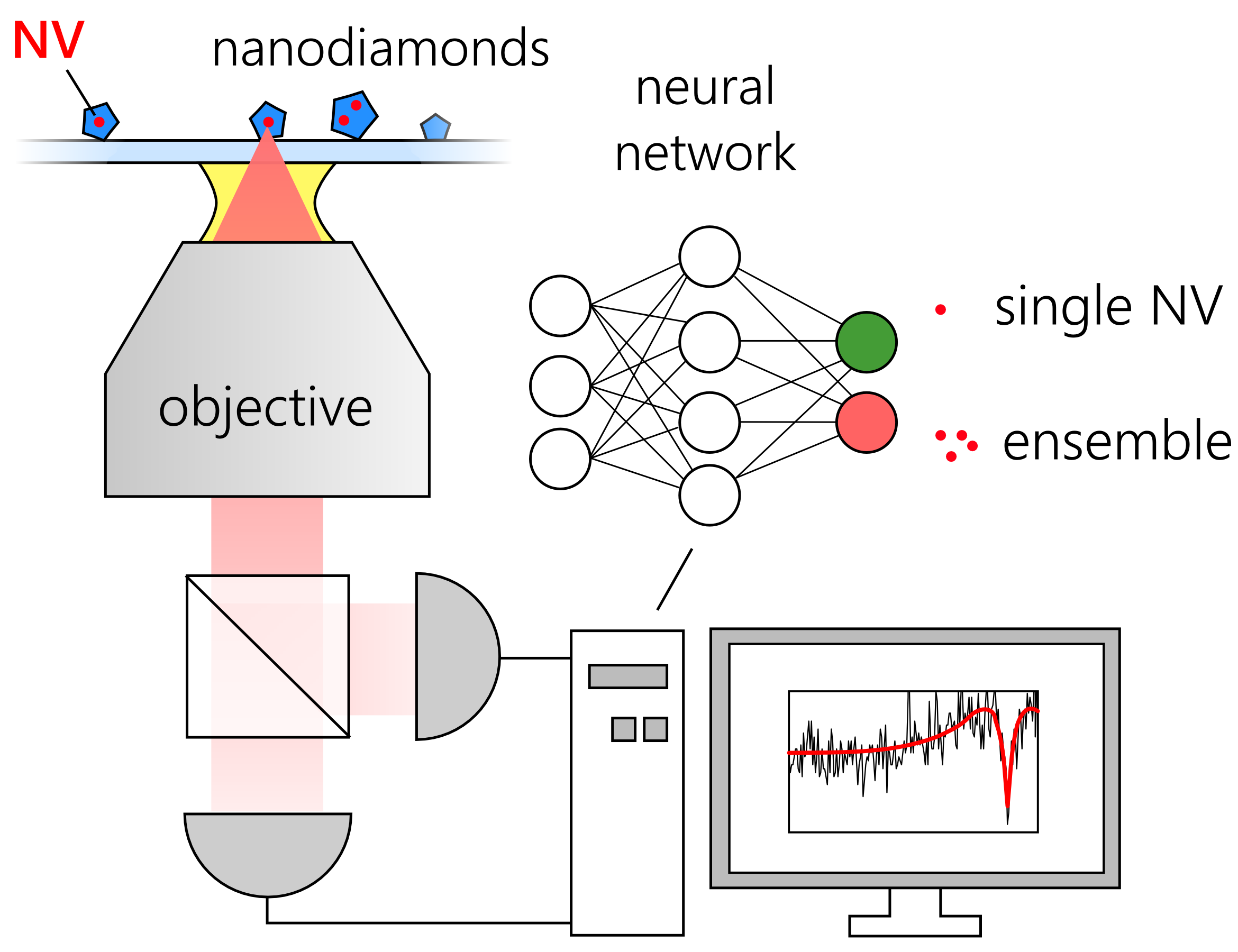
Rapid and deterministic nanoscale assembly of quantum emitters remains a daunting challenge for the realization of practical, on-chip quantum photonic devices. The major bottleneck is the time-consuming second-order photon autocorrelation measurements for the classification of solid-state quantum emitters into “single” and “non-single” photon sources during the quantum device assembly. We have adapted supervised machine learning algorithms to perform such classification in an efficient sub-second process based on sparse autocorrelation data. We demonstrate an ~80% fidelity of emitter classification based on datasets containing on average only one co-detection event per bin. In contrast, the conventional fitting classification method based on Levenberg-Marquardt fitting typically requires two-orders of magnitude longer collection times, and it fails entirely when applied to the same datasets. We anticipate that machine learning-based classification will provide a unique route to enable rapid and scalable assembly of quantum nanophotonic devices and can be directly extended to other quantum optical measurements, promising breakthroughs in quantum information, sensing and super-resolution microscopy.
Z.A. Kudyshev, S.I. Bogdanov, T. Isacsson, A.V. Kildishev, A. Boltasseva, and V. M. Shalaev, Adv. Quant. Technol., 3, 2000067 (2020)
21. On-chip single-layer integration of diamond spins with microwave and plasmonic channels

On-chip scalable integration represents a major challenge for practical quantum devices. One particular challenge is to implement on-chip optical readout of spins in diamond. This readout requires simultaneous application of optical and microwave fields along with an efficient collection of fluorescence. The readout is typically accomplished via bulk optics and macroscopic microwave transmission structures. We experimentally demonstrate an on-chip integrated structure for nitrogen‑vacancy (NV) spin-based applications, implemented in a single material layer with one patterning step. A nanodiamond with multiple NV centers is positioned at the end of the groove waveguide milled in a thick gold film. The gold film carries the microwave control signal while the groove waveguide acts as a fluorescence collector, partially filtering out the pump excitation. As a result, the device dimensions and fabrication complexity are substantially reduced. Our approach will foster further development of ultra-compact nanoscale quantum sensors and quantum information processing devices on a monolithic platform. NV center-based nanoscale sensors are the most promising application of the developed interface.
M. Y. Shalaginov, S. I. Bogdanov, A. S. Lagutchev, A. V. Kildishev, A. Boltasseva, and V. M. Shalaev, ACS Photonics 7, 2018 (2020)
20. Chip-compatible quantum plasmonic launcher
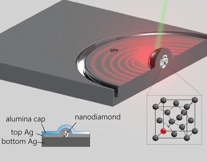
Integrated on-demand single-photon sources are critical for the implementation of photonic quantum information processing systems. To enable practical quantum photonic devices, the emission rates of solid-state quantum emitters need to be substantially enhanced and the emitted signal must be directly coupled to an on-chip circuitry. The photon emission rate speed-up is best achieved via coupling to plasmonic antennas, while on-chip integration can be easily obtained by directly coupling emitters to photonic waveguides. The realization of practical devices requires that both the emission speed-up and efficient out-coupling are achieved in a single architecture. Here, we propose a novel platform that effectively combines on-chip compatibility with high radiative emission rates, a quantum plasmonic launcher. The proposed launchers contain single nitrogen-vacancy (NV) centers in nanodiamonds as quantum emitters that offer record-high average fluorescence lifetime shortening factors of about 7000 times. Nanodiamonds with single NV are sandwiched between two silver films that couple more than half of the emission into in-plane propagating surface plasmon polaritons. This simple, compact, and scalable architecture represents a crucial step towards the practical realization of high-speed on-chip quantum networks.
C.-C. Chiang, S. I. Bogdanov, O. A. Makarova, X. Xu, S. Saha, D. Shah, D. Wang, A. S. Lagutchev, A. V. Kildishev, A. Boltasseva, and V. M. Shalaev, Adv. Opt. Mater., 8 2000889 (2020)
19. Ultrafast quantum photonics enabled by coupling plasmonic nanocavities to strongly radiative antennas
Quantum emitters coupled to plasmonic nanostructures can act as exceptionally bright sources of single photons. Plasmonic mode volumes supported by these nanostructures can be several orders of magnitude smaller than the cubic wavelength, which leads to dramatically enhanced light-matter interactions and drastically increased photon production rates. However, when increasing the light localization further, these deeply subwavelength modes may in turn hinder the fast outcoupling of photons into the free space. Plasmonic hybrid nanostructures combining a highly confined cavity mode and a larger antenna mode circumvent this issue. We establish the fundamental limits for quantum emission enhancement in such systems and find that the best performance is achieved when the cavity and antenna modes differ significantly in size. We experimentally support this idea by photomodifying a single-photon nanopatch antenna deterministically assembled around a nanodiamond known to contain a single nitrogen-vacancy (NV) center. As a result, the cavity mode shrinks, further shortening the NV fluorescence lifetime and increasing the single-photon brightness. Our analytical and numerical simulation results provide an intuitive insight into the operation of these emitter-cavity-antenna systems and show that this approach could lead to single-photon sources with emission rates up to hundreds of THz and efficiencies close to unity.
S.I. Bogdanov, O.A. Makarova, X. Xu, Z.O. Martin, A.S. Lagutchev, M. Olinde, D. Shah, S.N. Chowdhuri, A.R. Gabidullin, I.A. Ryzhikov, I.A. Rodionov, A.V. Kildishev, S.I. Bozhevolnyi, A. Boltasseva, V.M. Shalaev and J.B. Khurgin, Optica, 7, 463 (2020)
18. Deterministic integration of single nitrogen-vacancy centers into nanopatch antennas
Quantum emitters coupled to plasmonic nanoantennas produce single photons at unprecedentedly high rates in ambient conditions. This enhancement of quantum emitters’ radiation rate is based on the existence of optical modes with highly sub-diffraction volumes supported by plasmonic gap-nanoantennas. Nanoantennas with gap sizes on the order of few nanometers have been typically produced using various self-assembly or random assembly techniques. Yet, the difficulty of controllably fabricate nanoantennas with the smallest mode sizes coupled to pre-characterized single emitters until now has remained a serious issue plaguing the development of quantum plasmonic devices. We demonstrate the transfer of nanodiamonds with single nitrogen-vacancy (NV) centers to an epitaxial silver substrate and their subsequent deterministic coupling to plasmonic gap nanoantennas. Through fine control of the assembled nanoantenna geometry, a dramatic shortening of the NV fluorescence lifetime was achieved. We furthermore show that by preselecting NV centers exhibiting a photostable spin contrast, a coherent spin dynamics can be measured in the coupled configuration. The demonstrated approach opens unique applications of plasmon-enhanced quantum emitters for integrated quantum information and sensing devices.
S.I. Bogdanov, O.A. Makarova, A.S. Lagutchev, D. Shah, C.-C. Chiang, S. Saha, A.S. Baburin, I.A. Ryzhikov, I.A. Rodionov, A.V. Kildishev, A. Boltasseva and V.M. Shalaev, preprint available on arXiv at http://arxiv.org/abs/1902.05996
17. Superconductivity behavior in epitaxial TiN films points to surface magnetic disorder

We analyze the evolution of the normal and superconducting electronic properties in epitaxial TiN films as a function of the film thickness with high Ioffe-Regel parameter values. As the film thickness decreases, we observe an increase in the residual resistivity, which becomes dominated by diffusive surface scattering for d ≤ 20nm. At the same time, a substantial thickness-dependent reduction of the superconducting critical temperature is observed compared to the bulk TiN value. In such high-quality material films, this effect can be explained by a weak magnetic disorder residing in the surface layer. Our results suggest that surface magnetic disorder is generally present in oxidized TiN films.
N.A. Tovpeko, N.A. Titova, E.M. Baeva, A.V. Semenov, S. Saha, H. Reddy, S. Bogdanov, E.E. Marinero, V.M. Shalaev, A. Boltasseva, V.S. Khrapai, A.I. Kardakova, and G.N. Goltsman, Phys. Rev. Applied 12, 054001 (2019)
16. Overcoming quantum decoherence with plasmonics
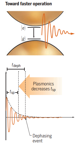
Single photons are the most suitable carriers of information for the implementation of quantum networks. Most optical quantum information scenarios require that photons be “coherent” or indistinguishable. Loss of coherence often occurs when light interacts with matter, which is needed to produce single photons and perform logical operations on them. One way to combat optical decoherence is to suppress noise in matter e.g. through cryogenic cooling. A targeted use of plasmonics (i.e. metal-based photonics) offers a different, arguably more attractive path. In this Perspective, we discuss the approach to achieve quantum optical coherence by dramatically speeding up light-matter interaction. We also outline strategies to minimize photon losses in metals.
S.I. Bogdanov, A. Boltasseva and V.M. Shalaev, Science, 364, 532 (2019)
15. Ultrabright room-temperature sub-nanosecond emission from single nitrogen-vacancy centers coupled to nano-patch antennas
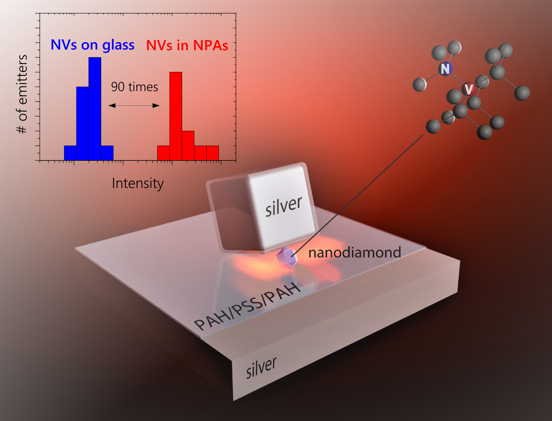
Single-photon emitters are intrinsically dim because they emit photons one by one, and these photons are separated on average by the characteristic time of spontaneous decay – the fluorescence lifetime. Using plasmonic nanoantennas, it is possible to shorten this lifetime by 100 or even 1000 times, which could make the emitters brighter. However, optical absorption in most plasmonic materials is several orders of magnitude stronger than in dielectrics. As a result, the increase in brightness in plasmonic nanoantennas has been far behind what the lifetime shortening suggests: most of the emission ends up being absorbed and never makes it into the far-field. We have employed epitaxial silver films with record-low losses from our collaborators in Moscow, Russia and crystalline silver nanocubes to fabricate single-photon nanoantennas. We used photostable nitrogen-vacancy centers in diamond as single-photon emitters. The resulting sources of single photons emit tens of millions of photons per second, making them the brightest ones operating at room temperature.
S.I. Bogdanov, M.Y. Shalaginov, A.S. Lagutchev, C.-C. Chiang, D. Shah, A.S. Baburin, I.A. Ryzhikov, I.A. Rodionov, A.V. Kildishev, A. Boltasseva, and V.M. Shalaev, Nano Letters, 18, 4837 (2018)

14. Hybrid Plasmonic Bullseye Antennas for Efficient Photon Collection
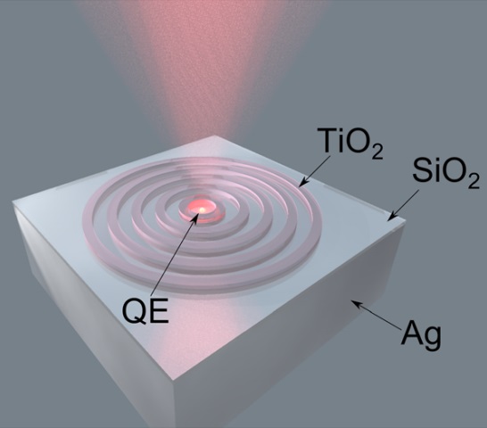
The fluorescence of nanoscale quantum emitters is intrinsically isotropic and therefore difficult to harvest. We have fabricated a plasmonic antenna consisting of an unprocessed flat protected silver layer and a bulls-eye titania grating. Using an AFM tip, we have placed a nanodiamond containing a nitrogen-vacancy center ensemble (NVE) into the center of the antenna. As a result, we have obtained highly directional (< 10° half-angle) emission from the NVE in a broad (600-700 nm) wavelength range.
S.K.H. Andersen, S. Bogdanov, Y. Xuan, O. Makarova, M.Y. Shalaginov, A. Boltasseva, V.M. Shalaev and S. Bozhevolnyi, ACS Photonics, 5, 692 (2018)
13. Patterned multilayer metamaterial for fast and efficient photon collection from dipolar emitters

The coupling of nanoscale optical emitters to a planar hyperbolic metamaterial results in a significant Purcell enhancement in a very broad wavelength range, unlike in the case of resonant antennas. However, in this case, most of the enhanced emission is lost inside the metamaterial, leading to poor collection efficiency (< 1% for the out-of-plane dipoles). To circumvent this issue, we numerically show that a simple circular corrugation in the metamaterial layer can improve the collection efficiency by 10 to 50 times from arbitrarily oriented dipoles and in a broad wavelength range (600-800 nm).
O.A. Makarova, M.Y. Shalaginov, S. Bogdanov, U. Guler, A. Boltasseva, A.V. Kildishev and V.M. Shalaev, Optics Letters 42, 3968 (2017)
12. Electron spin contrast of Purcell-enhanced nitrogen-vacancy ensembles in nanodiamonds
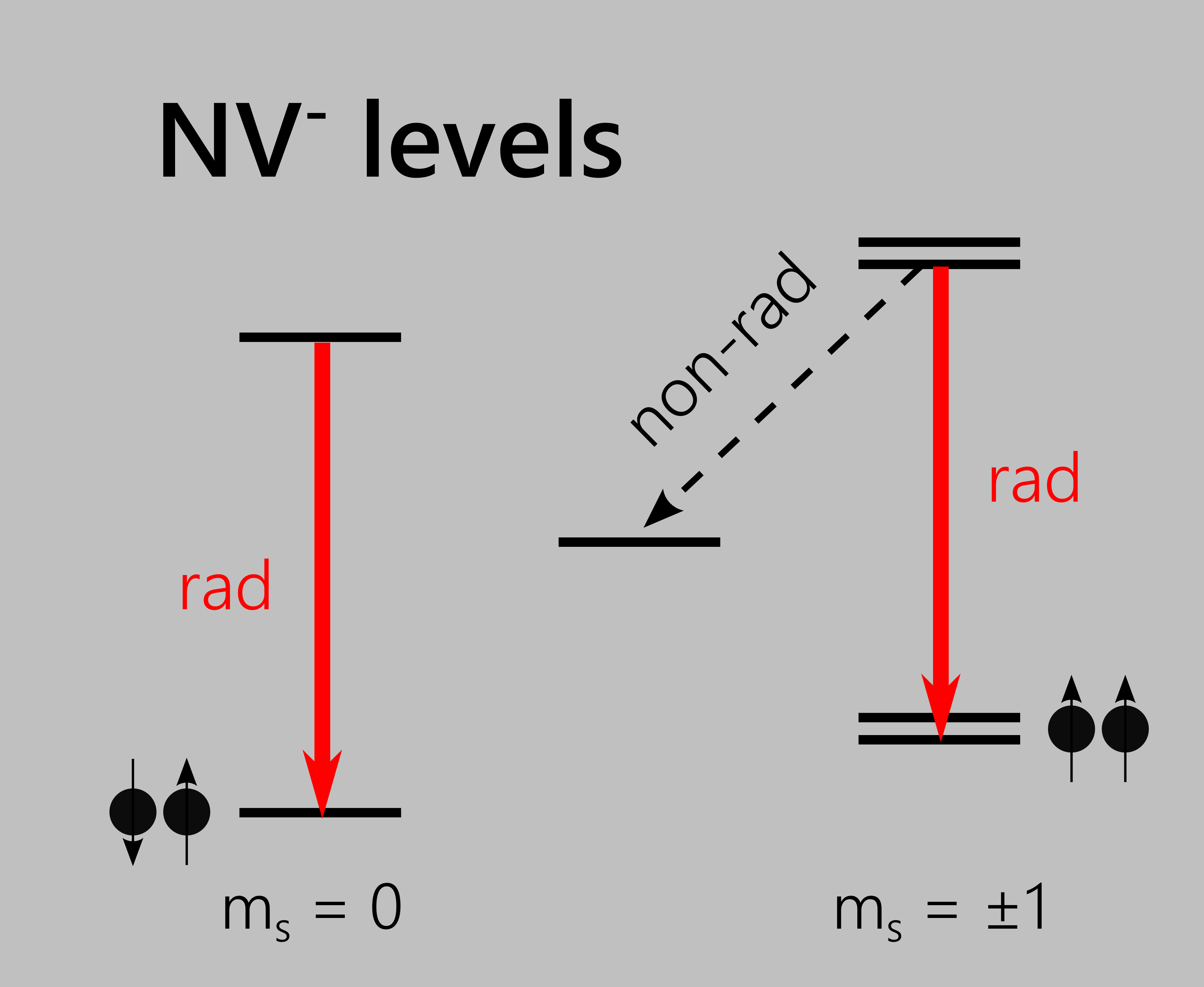
Nitrogen-vacancy centers in diamond allow for coherent spin-state manipulation at room temperature, which could bring dramatic advances to nanoscale sensing and quantum information technology. We introduce a method for the optical measurement of the spin contrast in dense nitrogen-vacancy (NV) ensembles. This method brings insight into the interplay between the spin contrast and fluorescence lifetime. We show that for improving the spin readout sensitivity in NV ensembles, one should aim at modifying the far-field radiation pattern rather than
enhancing the emission rate.
S. Bogdanov, M.Y. Shalaginov, P. Kapitanova, J. Liu, M. Ferrera, A. Lagutchev, P. Belov, J. Irudayaraj, A. Boltasseva and V. Shalaev, Physical Review B 96, 035146 (2017)
11. Material platforms for integrated quantum photonics

On-chip integration of quantum optical systems could be a major factor enabling photonic quantum technologies. While III-V materials have been shown to host most quantum photonic components, the issues of their intercompatibility, scalability and performance are far from being solved. Therefore, many material platforms are being examined to host the future quantum photonic computers and network nodes. We discuss the pros and cons of several platforms for realizing various elementary devices, compare the current degrees of integration achieved in each platform and review several composite platform approaches.
S. Bogdanov, M.Y. Shalaginov, A. Boltasseva and V.M. Shalaev, Optical Materials Express 7, 111 (2017)
10. Antimonide-based type-II superlattices – a superior candidate for the third generation of infarared imaging systems

Type II superlattices (T2SLs), a system of interacting multiquantum wells, were introduced by Nobel Laureate L. Esaki in the 1970s. Since then, this material system has drawn a lot of attention, especially for infrared detection and imaging. We present the current status of T2SL-based photodetectors and FPAs for imaging in different infrared regimes, from short wavelength to very long wavelength, and dual-band infrared detection and imaging, as well as the future outlook for this material system.
M. Razeghi, A. Haddadi, A.M. Hoang, G. Chen, S. Bogdanov, S.R. Darvish, F. Callewaert, P.R. Bijjam and R. McClintock, Journal of Electronic Materials 43(8), 2802 (2014)
9. Effect of sidewall surface recombination on the quantum efficiency in a Y2O3 passivated gated type-II InAs/GaSb long-infrared photodetector array
Yttrium oxide was applied to passivate a long-wavelength infrared type-II superlattice gated photodetector array, reducing the saturated gate bias by three times compared to a SiO2 passivated array. Besides effectively suppressing surface leakage, the gating technique enhanced the quantum efficiency of 100×100 micron size mesas from 51% to 57% by suppressing sidewall surface recombination.
G. Chen, A.M. Hoang, S. Bogdanov, A. Haddadi, S.R. Darvish and M. Razeghi, Applied Physics Letters 103, 223501 (2013).
8. Investigation of impurity in type-II InAs/GaSb superlattices via capacitance-voltage measurement
G. Chen, A.M. Hoang, S. Bogdanov, P.R. Bijjam, B.-M. Nguyen and M. Razeghi, Applied Physics Letters 103, 033512 (2013).
7. Surface leakage investigation via gated type-II InAs/GaSb long-wavelength infrared photodetectors
G. Chen, E.K. Huang, A.M. Hoang, S. Bogdanov, S.R. Darvish and M. Razeghi, Applied Physics Letters 101, 213501 (2012).
6. Advances in antimonide-based Type-II superlattices for infrared detection and imaging at the center for quantum devices
M. Razeghi, A. Haddadi, A.M. Hoang, E.K. Huang, G. Chen, S. Bogdanov, S.R. Darvish, F. Callewaert and R. McClintock, Infrared Physics and Technology, 59, 41 (2012).
5. Effect of contact doping on superlattice-based minority-carrier unipolar detectors
B.M. Nguyen, G. Chen, A.M. Hoang, S. Abdollahi Pour, S. Bogdanov, and M. Razeghi, Applied Physics Letters 99, 033501 (2011).
4. Surface leakage current reduction in long wavelength infrared type-II InAs/GaSb superlattice photodiodes
S. Bogdanov, B.M. Nguyen, A.M. Hoang and M. Razeghi, Applied Physics Letters 98, 183501 (2011).
3. Minority electron unipolar photodetectors based on type II InAs/GaSb/AlSb superlattices for very long wavelength infrared detection
B.M. Nguyen, S. Bogdanov, S. Abdollahi Pour, and M. Razeghi, Applied Physics Letters 95, 183502 (2009).
2. Demonstration of high performance long wavelength infrared type II InAs/GaSb superlattice photodiode grown on GaAs substrate
S. Abdollahi Pour, B.M. Nguyen, S. Bogdanov, E.K. Huang, and M. Razeghi, Applied Physics Letters 95, 173505 (2009).
1. Demonstration of midinfrared type-II InAs/GaSb superlattice photodiodes grown on GaAs substrate
B.M. Nguyen, D. Hoffman, E.K. Huang, S. Bogdanov, P.Y. Delaunay, M. Razeghi and M.Z. Tidrow, Applied Physics Letters 94, 223506 (2009).
